The new Galaxy S21 series of devices have been out commercially for a week now, and we’ve managed to get our hands on two Galaxy S21 Ultras – one with Qualcomm’s new Snapdragon 888 SoC, and one with Samsung’s new Exynos 2100 SoC. Both chipsets this year are more similar than ever, both now sporting similar CPU configurations, and both being produced on a new Samsung 5nm (5LPE) process node.
Ahead of our full device review of the Galaxy S21 Ultra (and the smaller Galaxy S21), today we’re focusing on the first test results of the new generation of SoCs, putting them through their paces, and pitting them against each other in the new 2021 competitive landscape.
The Snapdragon 888
| Qualcomm Snapdragon Flagship SoCs 2020-2021 | |||
| SoC | Snapdragon 865 |
Snapdragon 888 |
|
| CPU | 1x Cortex-A77 @ 2.84GHz 1x512KB pL2 3x Cortex-A77 4x Cortex-A55 4MB sL3 |
1x Cortex-X1 @ 2.84GHz 1x1024KB pL2 3x Cortex-A78 4x Cortex-A55 4MB sL3 |
|
| GPU | Adreno 650 @ 587 MHz | Adreno 660 @ 840MHz | |
| DSP / NPU | Hexagon 698
15 TOPS AI |
Hexagon 780
26 TOPS AI |
|
| Memory Controller |
4x 16-bit CH
@ 2133MHz LPDDR4X / 33.4GB/s 3MB system level cache |
4x 16-bit CH
@ 3200MHz LPDDR5 / 51.2GB/s 3MB system level cache |
|
| ISP/Camera | Dual 14-bit Spectra 480 ISP
1x 200MP or 64MP with ZSL 4K video & 64MP burst capture |
Triple 14-bit Spectra 580 ISP
1x 200MP or 84MP with ZSL 4K video & 64MP burst capture |
|
| Encode/ Decode |
8K30 / 4K120 10-bit H.265
Dolby Vision, HDR10+, HDR10, HLG 720p960 infinite recording |
8K30 / 4K120 10-bit H.265
Dolby Vision, HDR10+, HDR10, HLG 720p960 infinite recording |
|
| Integrated Modem | none (Paired with external X55 only) (LTE Category 24/22) (5G NR Sub-6 + mmWave) |
X60 integrated
(LTE Category 24/22) (5G NR Sub-6 + mmWave) |
|
| Mfc. Process | TSMC 7nm (N7P) |
Samsung 5nm (5LPE) |
|
Starting off with the new Snapdragon 888 SoC, Qualcomm’s new flagship model makes iterative steps this generation, with the biggest changes of the new design actually being in the form of the new Hexagon 780 accelerator, which fuses together traditional scalar and vector DSP operations with tensor execution engines within one single IP block.
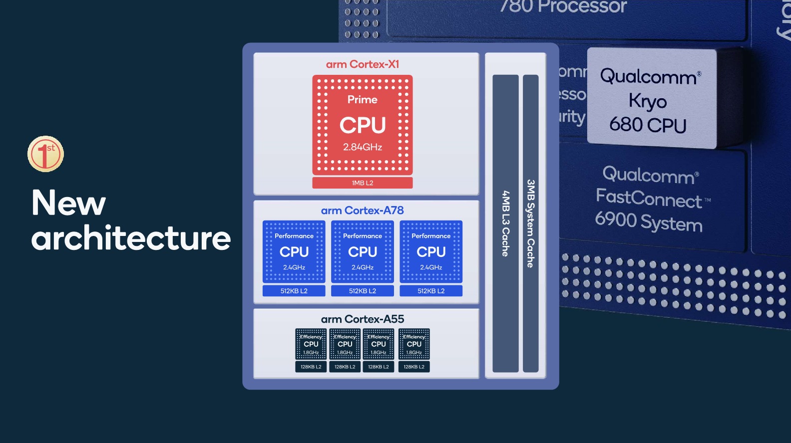
Of course, we’re also seeing upgrades elsewhere in the architecture, with the Snapdragon 888 being among the first SoCs to use Arm’s new Cortex-X1 CPU IP, promising large performance gains relative to last generation Cortex-A77 cores. The single X1 cores in the Snapdragon 888 clocks in at 2.84GHz – the same as the previous generation Snapdragon 865’s prime Cortex-A77 cores, and less than the 3.1GHz and 3.2GHz Snapdragon 865+ and recently announced Snapdragon 870 SoCs.
Alongside the X1, we find three Cortex-A78 cores at 2.42GHz, again the same clocks as the previous generation 865 SoCs, but this time around with double the L2 caches at 512KB.
The Cortex-A55 little cores remain identical this generation, clocking in at 1.8GHz.
Although we had been expecting 8MB L3 cache flagship SoCs this year, it does look like Qualcomm opted to remain at 4MB for this generation – but at least the company dons the X1 core with the maximum 1MB L2 cache configuration.
On the GPU side of things, Qualcomm’s new Adreno 660 GPU now clocks in up to a peak 840MHz – a whopping 43% higher frequency than the Snapdragon 865 GPU. The company’s performance claims here are also astonishing, promising a +35% boost in performance. We’ll have to see how this all ends up in terms of power consumption and long-term performance in the later dedicated GPU section.
What’s quite different for the Snapdragon 888 this year is that Qualcomm has moved from a TSMC N7P process node to Samsung’s new 5LPE node – the generally wildcard in this whole situation as we haven’t had any prior experience with this new 5nm node.
The Exynos 2100
| Samsung Exynos SoCs Specifications | |||
| SoC |
Exynos 990 |
Exynos 2100 |
|
| CPU | 2x Exynos M5 @ 2.73GHz 2MB sL2 3MB sL3 2x Cortex-A76 4x Cortex-A55 1MB sL3 |
1x Cortex-X1 @ 2.91GHz 1x512KB pL2 3x Cortex-A78 4x Cortex-A55 4MB sL3 |
|
| GPU | Mali G77MP11 @ 800 MHz | Mali G78MP14 @ 854 MHz | |
| Memory Controller |
4x 16-bit CH
@ 2750MHz LPDDR5 / 44.0GB/s 2MB System Cache |
4x 16-bit CH
@ 3200MHz LPDDR5 / 51.2GB/s 6MB System Cache |
|
| ISP | Single: 108MP Dual: 24.8MP+24.8MP |
Single: 200MP Dual: 32MP+32MP (Up to quad simultaneous camera) |
|
| NPU | Dual NPU + DSP + CPU + GPU 15 TOPs |
Triple NPU + DSP + CPU + GPU 26 TOPs |
|
| Media | 8K30 & 4K120 encode & decode H.265/HEVC, H.264, VP9 |
8K30 & 4K120 encode & 8K60 decode H.265/HEVC, H.264, VP9 |
|
| Modem | Exynos Modem External
(LTE Category 24/22) (5G NR Sub-6) (5G NR mmWave) |
Exynos Modem Integrated
(LTE Category 24/18) (5G NR Sub-6) (5G NR mmWave) |
|
| Mfc. Process | Samsung 7nm (7LPP) |
Samsung 5nm (5LPE) |
|
On the Samsung LSI side of things, we find the brand-new Exynos 2100. Unlike the Snapdragon 888’s more incremental changes in terms of SoC design, the new Exynos is a rather large departure for Samsung’s SoC division as this is the first flagship design in many years that no longer uses Samsung’s own in-house CPU microarchitecture, but rather reverts back to using Arm Cortex cores, which in this case is also the new Cortex-X1 and Cortex-A78 cores.
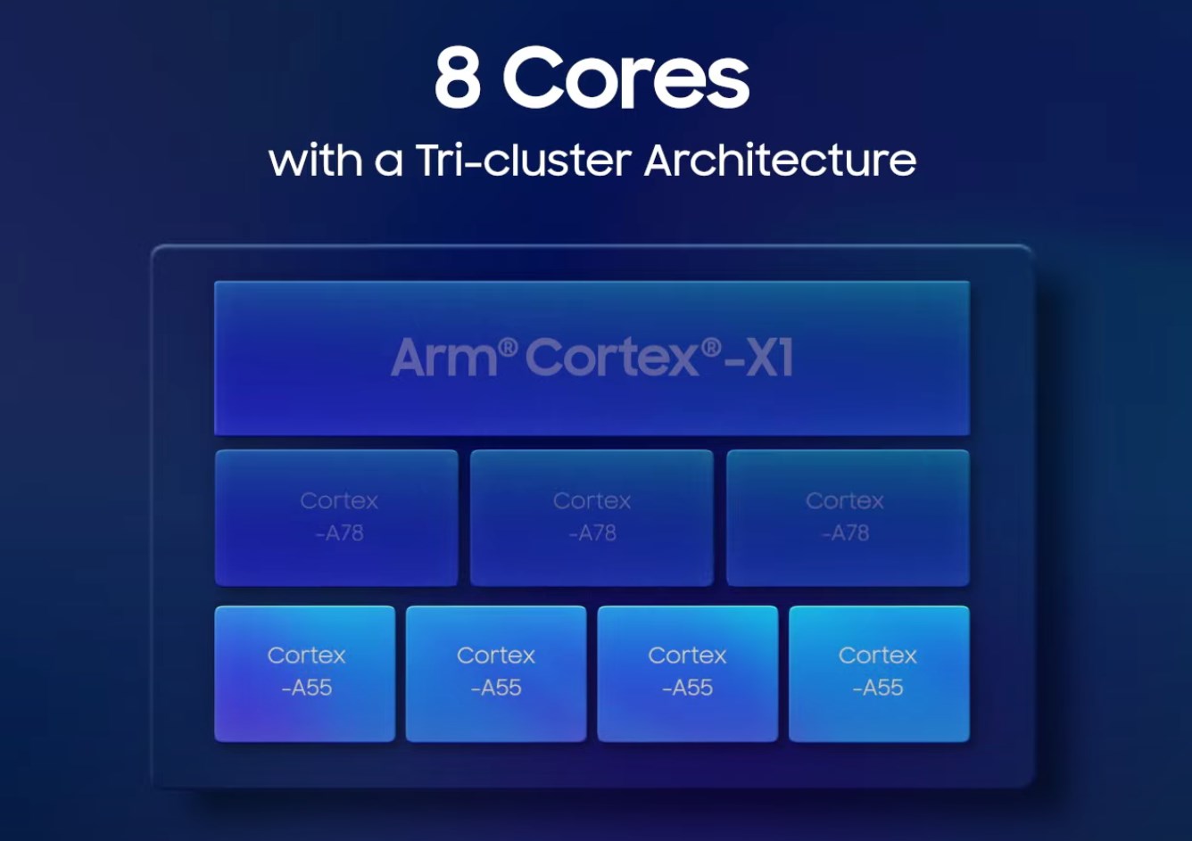
From a high-level, the CPU configuration of the Exynos 2100 looks nigh identical to that of the Snapdragon 888, as both are 1+3+4 designs with X1, A78 and A55 cores. The differences are in the details:
The X1 cores on the Exynos 2100 clock slightly higher at up to 2.91GHz, while the Cortex-A78 clock in significantly higher than the Snapdragon as they reach 2.81GHz. The Cortex-A55 cores are also quite aggressive in terms of frequency as they now reach 2.20GHz – so overall across the board higher clocks than the Snapdragon variant.
Where the Exynos isn’t as aggressive though is in its cache configurations. Most importantly, the X1 cores here only feature 512KB of L2 cache, which is a bit weird given the all-out-performance philosophy of the new CPU. The Cortex-A78s also see the usage of 512KB L2 caches, while the little A55 cores feature 64KB L2’s – less than the Snapdragon counterparts.
Much like the Snapdragon, the L3 cache also falls in at 4MB rather than the 8MB we would have hoped for this generation, however Samsung does surprise us with the usage of an estimated 6-8MB system level cache, up from the 2MB design in the Exynos 990.
On the GPU side of things, we see a Mali-G78MP14 at up to 854MHz. That’s 27% more cores and 6.7% higher frequency, and the company is also boasting massive performance gains as it touts a 40% generational improvement.
Let them fight
In today piece, we’ll be mostly focusing around CPU and GPU performance, as an especially interesting comparison will be to see how the two designs do against each other, given that they both now use Arm’s newest Cortex-X1 cores and both are sporting the same manufacturing node.
The GPU comparisons will also be interesting – and maybe quite controversial, as the results won’t be what many people will have been expecting.
While we would have liked to showcase AI performance of the two SoCs – unfortunately the software situation on the Galaxy S21’s right now means that neither SoC are fully taking advantage of their new accelerators, so that’s a topic to revisit in a few months’ time once the proper frameworks have been updated by Samsung.
Table Of Contents
- The Snapdragon 888 & Exynos 2100
- 5nm / 5LPE: What Do We Know?
- Memory Subsystem & Latency: Quite Different
- SPEC - Single Threaded Performance & Power
- Mixed-Usage Power & Preliminary Battery Life
- GPU Performance & Power: Very, Very Hot
- Conclusion & End Remarks
Starting off with the biggest new change of this generation, both the Snapdragon 888 and the Exynos 2100 are manufactured on Samsung’s new 5nm process node, which is the biggest unknown in today’s comparison.
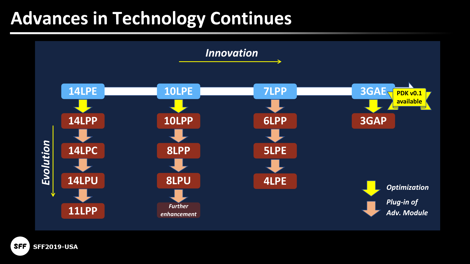
What’s important to remember is that although Samsung calls this node 5nm, its design and characteristics are more similar to that of their 7nm node. Key new characteristics of the new node here are the reintroduction of single diffusion breaks (SDB) on an EUV process node, as well as slight changes in the cell libraries of the process.
| Advertised PPA Improvements of New Process Technologies Data announced by companies during conference calls, press briefings and in press releases |
||||||
| 7LPP vs 10LPE |
6LPP vs 7LPP |
5LPE vs 7LPP |
3GAE vs 7LPP |
|||
| Power | 50% | lower | 20% | 50% | ||
| Performance | 20% | ? | 10% | 35% | ||
| Area Reduction | 40% | ~9% | <20% | 40% | ||
Per Samsung’s own numbers, the foundry claims that 5LPE is either 20% lower power than 7LPP, or 10% more performance. These are actually quite important figures to put into context, particularly when we’re comparing designs which are manufactured on TSMC’s process nodes.
In least year’s review of the Galaxy S20 series and the Exynos 990 and Snapdragon 865 SoCs, an important data-point that put things into context was Qualcomm’s Snapdragon 765 SoC which was also manufactured on Samsung’s 7LPP node, and featuring Cortex-A76 cores. In that comparison we saw that The Exynos 990 and the Snapdragon 765’s A76 cores behaves very similarly in terms of power consumption, however they fell behind TSMC-based Cortex-A76 cores by anywhere from 20% to 30%.
In that context, Samsung’s 5LPE process node improving power by 20% would mean they’d only be catching up with TSMC’s 7nm nodes.
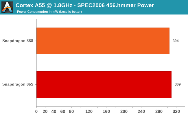
An interesting comparison to make – and probably one of the rare ones we’re actually able to achieve today, is the comparison between the Cortex-A55 cores inside of both the Snapdragon 865 and the new Snapdragon 888. Both SoCs feature the same IP cores, clock them at the same 1.8GHz frequency, and both feature the same amount of L2 cache, with their only real difference being their process nodes.
Using SPEC’s 456.hmmer – because it’s a workload that primarily resides in the lower cache hierarchies and thus, we avoid any impact of the possibly different memory subsystem, we can see that both SoCs’ power consumption indeed is almost identical, with performance also being identical with a score of 6.84 versus 6.81 in favour of the new Snapdragon 888.
So at least at first glance, our theory that Samsung’s 5LPE merely just catches up with the power consumption and power efficiency of TSMC’s N7/N7P nodes seems to be valid – at least at these frequencies.

Further interesting data is the voltage curves of the CPUs on the Exynos 2100. I’ve extracted the frequency voltages tables of both my devices, a regular S21 and an S21 Ultra, with the above curves being the better binned chip inside of the smaller S21.
Generationally, Samsung seems to have been able to greatly reduce voltages this generation. On the Cortex-A55 cores, the cores now only require 800mV at 2GHz whilst the Exynos 990 last year in our review unit they required over 1050mV. Similarly, although the comparison isn’t apples-to-apples, the Cortex-A78 cores at 2.5GHz only require 862mV, while the Cortex-A76 cores of the previous generation required also 1050mV.
What’s also very interesting to see is the voltage curves of the Cortex-X1 cores versus the Cortex-A78 cores: they’re both nigh identical to each other, which actually lines up with Arm’s claims that the new X1 cores have the same frequency capabilities as the A78 cores, only being larger and increasing their power consumption linearly in relation to their frequency.
Samsung’s frequency tables indicate that they had been testing the A55 up to 2.6GHz, and the X1 and A78 cores up to 3.2GHz – however voltages here are quite higher and it’s also likely SLSI wouldn’t have been able to achieve similar chip yields.
Unfortunately, I wasn’t able to extract data from my Snapdragon 888 S21 Ultra, so I can’t tell exactly where it falls in terms of voltages compared to the Exynos 2100. One thing I can confirm as being quite different between the two SoCs is that Samsung does actually give the Exynos 2100’s Cortex-X1 core its own dedicated voltage rail and PMIC regulator, while the Snapdragon 888 shares the same voltage rail across the X1 and A78 cores. In theory, that could mean that in more mixed-thread workloads, the Exynos has the opportunity to be more power efficiency than the Snapdragon 888.
Generally, the one thing I want people to take away here is that although Samsung calls this their 5nm node, it’s quite certain that it will not perform the same as TSMC’s 5nm node. Usually we don’t care about density all too much, however performance and power efficiency are critical aspects that effect the silicon and the end-products’ experiences.
The memory subsystem comparisons for the Snapdragon 888 and Exynos 2100 are very interesting for a few couple of reasons. First of all – these new SoCs are the first to use new higher-frequency LPDDR5-6400 memory, which is 16% faster than that of last year’s LPDRR5-5500 DRAM used in flagship devices.
On the Snapdragon 888 side of things, Qualcomm this generation has said that they have made significant progress in improving memory latency – a point of contention that’s generally been a weak point of the previous few generations, although they always did keep improving things gen-on-gen.
On the Exynos 2100 side, Samsung’s abandonment of their custom cores also means that the SoC is now very different to the Exynos 990. The M5 used to have a fast-path connection between the cores and the memory controllers – exactly how Samsung reimplemented this in the Exynos 2100 will be interesting.
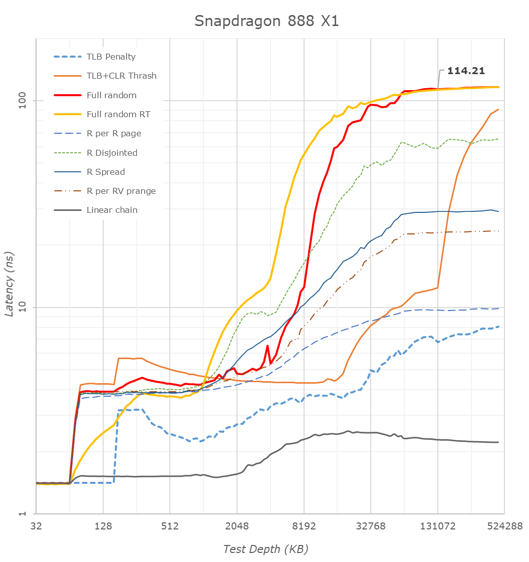
Starting things off with the new Snapdragon 888, we are seeing some very significant changes compared to the Snapdragon 865 last year. Full random memory latency went down from 138ns to 114ns, which is a massive generation gain given that Arm always quotes that 4ns of latency equals 1% of performance.
Samsung’s Exynos 2100 on the other hand doesn’t look as good: At around 136ns at 128MB test depth, this is quite worse than the Snapdragon 888, and actually a regression compared to the Exynos 990 at 131ns.
Looking closer at the cache hierarchies, we’re seeing 64KB of L1 caches for both X1 designs – as expected.
What’s really weird though is the memory patterns of the X1 and A78 cores as they transition from the L2 caches to the L3 caches. Usually, you’d expect a larger latency hump into the 10’s of nanoseconds, however on both the Cortex-X1 and Cortex-A78 on both the Snapdragon and Exynos we’re seeing L3 latencies between 4-6ns which is far faster than any previous generation L3 and DSU design we’ve seen from Arm.
After experimenting a bit with my patterns, the answer to this weird behaviour is quite amazing: Arm is prefetching all these patterns, including the “full random” memory access pattern. My tests here consist of pointer-chasing loops across a given depth of memory, with the pointer-loop being closed and always repeated. Arm seems to have a new temporal prefetcher that recognizes arbitrary memory patterns and will latch onto them and prefetch them in further iterations.
I re-added an alternative full random access pattern test (“Full random RT”) into the graph as alternative data-points. This variant instead of being pointer-chase based, will compute a random target address at runtime before accessing it, meaning it’ll be always a different access pattern on repeated loops of a given memory depth. The curves here aren’t as nice and they aren’t as tight as the pointer-chase variant because it currently doesn’t guarantee that it’ll visit every cache line at a given depth and it also doesn’t guarantee not revisiting a cache line within a test depth loop, which is why some of the latencies are lower than that of the “Full random” pattern – just ignore these parts.
This alternative patterns also more clearly reveals the 512KB versus 1MB L2 cache differences between the Exynos’ X1 core and the Snapdragon X1 core. Both chips have 4MB of L3, which is pretty straightforward to identify.
What’s odd about the Exynos is the linear access latencies. Unlike the Snapdragon whose latency grows at 4MB and remains relatively the same, the Exynos sees a second latency hump around the 10MB depth mark. It’s hard to see here in the other patterns, but it’s also actually present there.
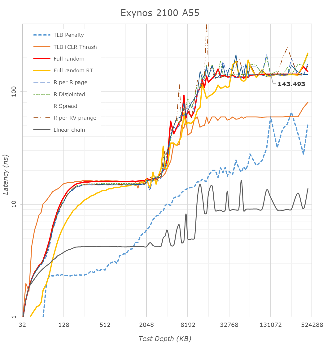
This post-4MB L3 cache hierarchy is actually easier to identify from the perspective of the Cortex-A55 cores. We see a very different pattern between the Exynos 2100 and the Snapdragon 888 here, and again confirms that there’s lowered latencies up until around 10MB depth.
During the announcement of the Exynos 2100, Samsung had mentioned they had improved and included “better cache memory”, which in context of these results seems to be pointing out that they’ve now increased their system level cache from 2MB to 6MB. I’m not 100% sure if it’s 6 or 8MB, but 6 seems to be a safe bet for now.
In these A55 graphs, we also see that Samsung continues to use 64KB L2 caches, while Qualcomm makes use of 128KB implementations. Furthermore, it looks like the Exynos 2100 makes available to the A55 cores the full speed of the memory controllers, while the Snapdragon 888 puts a hard limit on them, and hence the very bad memory latency, similarly to how Apple does the same in their SoCs when just the small cores are active.
Qualcomm seems to have completely removed access of the CPU cluster to the SoC’s system cache, as even the Cortex-A55 cores don’t look to have access to it. This might explain why the CPU memory latency this generation has been greatly improved – as after all, memory traffic had to do one whole hop less this generation. This also in theory would put less pressure on the SLC, and allow the GPU and other blocks to more effectively use its 3MB size.
Moving onto performance of the new CPU cores, something I’ve actually been quite excited about this generation, particularly because this year we hadn’t been able to do a proper in-depth performance preview of the Snapdragon 888 like we usually do on previous years.
Before we go into the results, I wanted to point out some discrepancies between the Exynos 2100 and Snapdragon 888 Galaxy S21 Ultra devices, particularly regarding clock frequencies under load: I’ve noted that the Exynos 2100 CPUs are extremely prone to throttling, in a quite drastic fashion compared my Snapdragon 888 unit. When tracking the average frequencies under SPEC, benchmarking the Exynos 2100 S21 Ultra under my typical peak performance conditions where I place the phone over a 140mm fan to keep it cool, the X1 cores were still throttling quite significantly even though the phone was only luke-warm.
The following are precise mean frequencies for the SPEC workloads, both under my usual fan-cooled conditions, as well as putting the S21 Ultra in my freezer:
| Cortex-X1 Average Workload Frequency | ||||
| S21 Ultra (Exynos 2100) Fan |
S21 Ultra (Exynos 2100) Freezer |
S21 Ultra (Snapdragon 888) Fan |
||
| 400.perlbench | 2613 | 2845 | 2826 | |
| 401.bzip2 | 2690 | 2904 | 2841 | |
| 403.gcc | 2688 | 2905 | 2839 | |
| 429.mcf | 2744 | 2912 | 2841 | |
| 445.gobmk | 2701 | 2908 | 2841 | |
| 456.hmmer | 2534 | 2752 | 2841 | |
| 458.sjeng | 2684 | 2912 | 2841 | |
| 462.libquantum | 2469 | 2857 | 2841 | |
| 464.h264ref | 2602 | 2901 | 2841 | |
| 471.omnetpp | 2756 | 2912 | 2842 | |
| 473.astar | 2667 | 2909 | 2841 | |
| 483.xalancbmk | 2668 | 2909 | 2841 | |
| 433.milc | 2369 | 2759 | 2842 | |
| 444.namd | 2603 | 2912 | 2841 | |
| 447.dealII | 2721 | 2889 | 2841 | |
| 450.soplex | 2573 | 2883 | 2841 | |
| 453.povray | 2544 | 2769 | 2841 | |
| 470.lbm | 2273 | 2628 | 2812 | |
| 482.sphinx3 | 2437 | 2709 | 2747 | |
The fan-cooled results are quite horrible, with the chip not sustaining the full 2.91GHz for any of the workloads. In this situation, in fact most of the tests barely run at 2912MHz, with most of the time the X1 cores being resident at 2600 or 2496MHz, with many tests going down to 2184MHz for periods of time.
Putting the device in the freezer (with a sock around the bottom part of the phone as to not damage the battery from it getting too cold), resulted in skin temperature hot-spots of around 6 to 10°C. Even under such unrealistic test conditions, the phone wasn’t able to sustain its peak frequency for many workloads, which is quite puzzling and worrying.
This Exynos S21 Ultra unit was quite unlucky in terms of its chip bin as the CPUs received ASV bins of 2, 2, 2 across the little, middle, and big cores. I’ve got another regular Galaxy S21 with another Exynos chip, which had slightly better bins of 4, 4, 3. While this device performed better and was slightly more efficient than the S21 Ultra, it was still significantly worse than the Snapdragon 888 Galaxy S21 Ultra, which had no issues to sustain near its 2841MHz peak frequency for the vast majority of workloads.
The following results are from the freezer-run Exynos S21 Ultra, as we’re attempting to analyse peak performance and the X1 cores themselves as well.
We use SPEC2006 for mobile devices still as it’s still relevant and we have a good understanding of the workloads. The benchmark is deprecated in favour of SPEC2017, which we hope to move to in the coming months. For the Android devices, this data-set is on a new NDK 22 compile as it resolves some performance discrepancies in our past data. We run simple and straightforward -Ofast flags.

In SPECint2006, we can see the new Cortex-X1 cores in both the Snapdragon 888 and Exynos 2100 perform a notch above the previous generation A77-cores, with particularly some larger jumps in tests such as 403.gcc and 464.h264ref.
The Snapdragon 888 in the majority of tests is able to take the lead, even though for the integer benchmarks the Exynos 2100 was mostly able to retain frequencies near 2.9GHz.
Qualcomm’s lower latency memory subsystem, as well as the advantage of the 1MB L2 cache are quite obvious here as it’s able to overcome, and outpace the clock frequency differences.
It’s to be noted that HiSilicon’s Kirin 9000 is still able to keep up with the new chips in quite a few of the workloads – the Kirin’s 3.13GHz clock frequency as well as an outstanding memory subsystem fall in its favour.
In terms of power and efficiency, it’s very obvious that the Exynos 2100 falls behind the Snapdragon 888. The chip uses more power, and it being slower, means it’s also taking up more energy to complete the tasks.
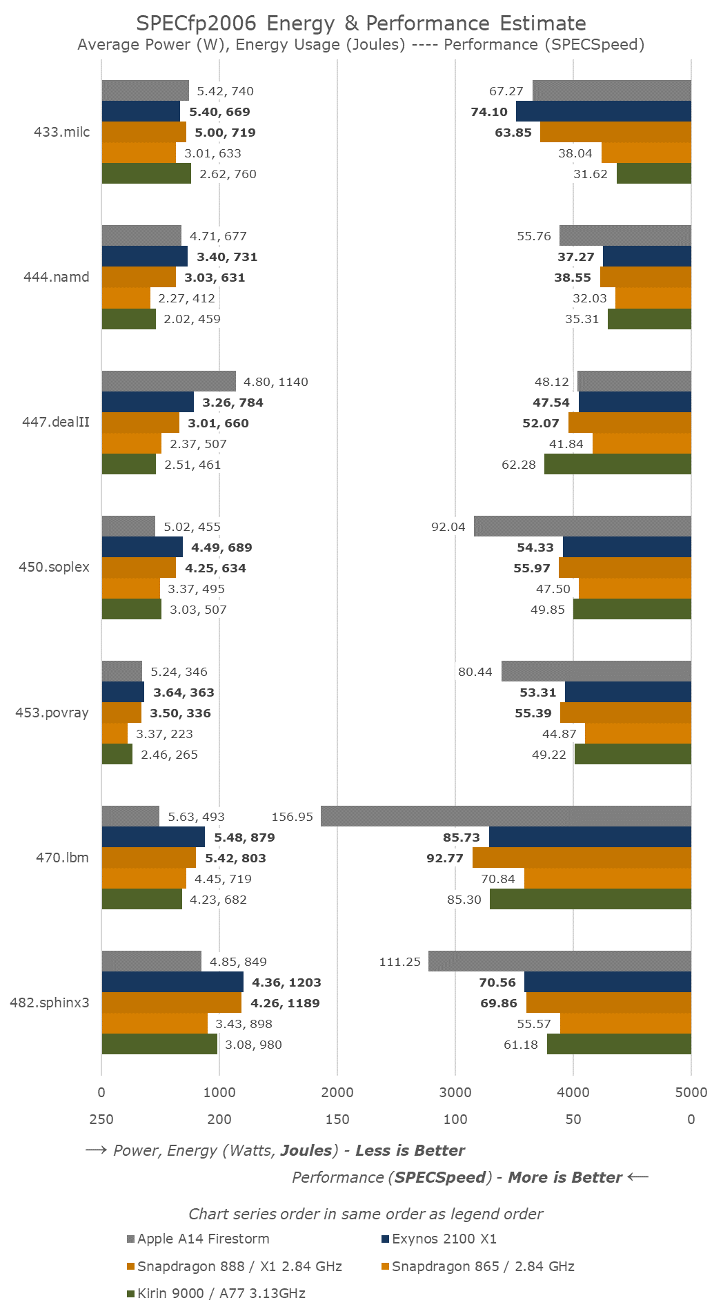
In SPECfp2006, the Exynos 2100 actually manages to score a few wins against the Snapdragon 888, but again falls behind in others as it has to throttle.
In 433.milc, the new X1 chips are posting gargantuan generational performance bumps, but which comes at a cost of power consumption in excess of 5W – whatever Arm did here this generation, it caught up and surpassed Apple in this one test.
For more extensive performance comparisons to past SoCs, such as the Exynos 990 I’ve updated our historical SPEC mobile data-set in the above large graph.
In the aggregate results scores, there’s a multitude of points we need to analyse.
Starting off with the Exynos 2100 – generationally, the new X1 cores and the Exynos 2100 are able to beat the Exynos 990 and the M5 cores by 27% and 25% in the integer and floating-point results. Samsung had officially stated the new SoC would be 19% faster in single-threaded scenarios – which I immediately through of as suspect as the improvements should be larger than that. I’m glad that the marketing was overly conservative and that my initial instinct was correct here. Although the X1 cores don’t use much different power consumption compared to the M5 cores, because of their increased performance, they are more energy efficient, using 23% and 18% less energy than the M5.
Looking at those figures though, they seem quite a bit odd, as they’re not that great as we had expected from the X1 cores, especially since this is also on a process node upgrade. Wouldn’t the cancelled M6 cores still have been competitive here?
The Snapdragon 888 results put things into context – it’s 5.1% and 1.6% faster than the Exynos 2100, however it’s also less power hungry, using 10% less power, resulting in being 14% more energy efficient. That’s not a large difference, but still sizeable given it’s the same CPU IP on the same process node.
Against the Snapdragon 865, the Snapdragon 888’s X1 cores are 23.8% and 29.2% faster. Because the cores are clocked at the same frequency, that’s also the generational IPC improvement that we’ve seen out of the new X1 cores. On the floating-point side, that essentially matches Arm’s 30% projection, however on the integer side it’s a few percentage points short – which is reasonable given that Arm’s figures had been projected with 8MB L3 cache implementations which we didn’t see this generation.
Energy efficiency of the Snapdragon 888 is slightly worse than that of the Snapdragon 865+, which means that battery life should be good this generation.
The Cortex-A78 cores of the Snapdragon 888 are 4.9% and 8.9% faster than the Cortex-A77 middle cores of the Snapdragon 865. The power consumption comparison here isn’t apples-to-apples due to the new cores doubling up on the L2 cache. Arm states the A78 has an +7% IPC improvement and a -4% power reduction versus the A77. The Snapdragon 888’s middle cores however use +24% more power. Excluding the theory that that doubled L2 cache significantly raises power, we’re probably still seeing a notable process node power efficiency difference between Samsung’s 5LPE node and TSMC’s N7P node, with the Samsung node still falling behind.
This power efficiency difference can also be seen in the Cortex-A78 cores of the Exynos 2100. At 2.81GHz, they’re near the 2.84GHz A77 cores of the Snapdragon 865 – both having 512KB L2 caches. The Exynos’ middle cores here actually outperform the previous Snapdragon’s performance cores by 8 and 13%, they however use 35% more power to do so, which is a whole damn lot. In fact, the throttling behaviour on the Exynos wasn’t just limited to the X1 cores, as under normal conditions even these middle A78 cores had to ramp down from their peak frequencies.
This behaviour of these new designs using quite large amounts of power at these higher frequencies, however being seemingly similar power to TSMC’s process nodes at lower frequencies, points out to me that the 5LPE node has lower performance than TSMC’s N7P node. The fact that the Kirin 9000 here is still competitive in terms of performance, but at significant lower power and better energy efficiency, also points out that the N5 node is well superior to Samsung’s offering.
Generally, we can’t do much about the process – especially if TSMC isn’t able to produce enough volume to satisfy both Apple as well as Qualcomm at the same time. Today’s performance and efficiency figures also fell below our projected targets of the X1 cores. Lower frequencies and smaller caches are primary reasons as to why. I find it weird from both Qualcomm as well as SLSI to have employed 4MB L3 caches. SLSI has in the last few years wasted a ton of silicon on their custom cores, so them skimping out even on the L2 cache here on the X1 is a really weird change of philosophy. Qualcomm did a better job, but also not as aggressive as you’d expect from a company which wants to acquire Nuvia in order to strengthen their CPU portfolio.
We haven’t had both Galaxy S21 Ultra devices long enough to do our more extensive battery life testing routines, however I did run some more power analysis on the more compute-heavy PCMark suite as well as some battery life numbers at 120Hz.
I’ll start off with some power profiling – these figures are generally within 5% margin of error accurate in terms of power usage at the battery level but are measured as input power into device as this allows us much higher resolution data sampling, without actually dismantling the phones.
I put the devices to minimum brightness to minimise screen power attribution in the power figures, with the devices set to 120Hz mode and a lamp shining on them to enable the 120Hz VRR/LFD power savings on the display. Both devices are in their default performance modes.
Galaxy S21 Ultra - Snapdragon 888
The Snapdragon 888’s power chart looks relatively straightforward here, with the different sections corresponding to the different sub-tests in PCMark. We see a varied amount of activity with clear activity spikes and corresponding power spikes when the SoC had to do computations.
Instantaneous peak power is around the 9W mark, which should be mostly due to the Cortex-X1 cores of the chip running alongside the Cortex-A78 cores.
Galaxy S21 Ultra - Exynos 2100
The Exynos chart looks generally similar, which is no surprise given that it’s the same workload. What’s more interesting about the Exynos though is that it has much larger power spikes, up to 14W, which is notably more than the Snapdragon. The Cortex-A78 cores on the Exynos run much higher frequency and power than on the Snapdragon, and together with the higher power draw of the X1 cores, it makes sense that the Exynos’ instantaneous power is considerably higher when all the cores are under load.
The photo editing section of the test is very intriguing as the power profile is very different to that of the Snapdragon. This RenderScript section should be accelerated by the GPU, and here we see the Exynos’ baseline power goes up significantly compared to the Snapdragon for the majority of the test. This is almost 1W in magnitude – I really wonder what’s happening here under the hood and where that power comes from – maybe the GPU doesn’t have as fine-grained power gating or DVFS?
| Galaxy S21 Ultra Power Usage in PCMark Minimum Brightness, 120Hz, Default Performance Mode |
|||
| Snapdragon 888 Score Power Usage |
Exynos 2100 Score Power Usage |
Difference Exynos vs Snapdragon |
|
| Idle Score Screen | 759 | 797 | 4.8% |
| Web-browsing | 12935
1309mW |
13159
1471mW |
+1.1%
+11.0% |
| Video Editing | 7866
2437mW |
6576
2998mW |
-16.4%
18.7% |
| Writing 2.0 | 12966
1556mW |
15370
2054mW |
+18.5%
24.2% |
| Photo Editing | 26884
881mW |
32385
1723mW |
+20.4%
48.9% |
| Data Manipulation | 9918
1450mW |
8930
1803mW |
-10%
19.6% |
Tabulating the PCMark test scores with the respective power figures across both Galaxy S21 Ultras, we see a few trends.
Performance wise, surprisingly enough, the Exynos has a few sub-tests where it outperforms the Snapdragon, notably in the Web-browsing, Writing and Photo editing tests. The Writing subtest particularly shows a +18% advantage in favour of the Exynos, while it loses more notably in the more single-threaded bound Data Manipulation test.
What’s also notable is that the Exynos’ power consumption is quite higher, across the board on all tests. The Photo Editing test aside where it has a 49% power disadvantage (which is actually high if we were to account for baseline device power), the rest of the test should be apples-to-apples CPU comparisons. We’re seeing roughly +15-20% device power disadvantages, and when account for baseline, this actually grows to around 18-35%. The Exynos does showcase a performance advantage in some of the tests, but not enough to make up for the increased power, meaning perf/W is lower.
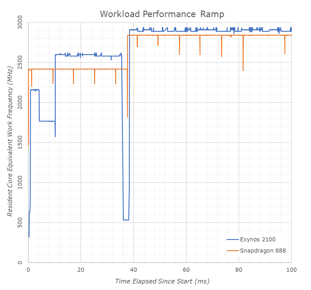
Looking at the DVFS of the two chips, we see that they’re generally reaching peak performance at roughly the same time in around 37-38ms. The Snapdragon 888 will schedule a workload directly on the A78 cores at 2.41GHz during that time before ramping up to the X1 cores at 2.84GHz. The Exynos starts off on the A55 cores at idle frequencies around 400-624MHz for 900µs, ramping up to 2210MHz for 4.2ms, before migrating onto the Cortex-A78 cores which start at 1768MHz and ramp up to 2600MHz. Oddly enough, when migrating to the X1 cores the scheduler seems to have troubles migrating the load as the cores run at the idle 533MHz before realising they have work to do and ramp up to the maximum 2.91GHz.
What’s interesting about the Exynos here is that for single-threaded workloads it doesn’t actually visit the A78’s max frequencies – which is actually a benefit for power efficiency and makes the SoC behave more like the Snapdragon counterparts even though is has higher peak frequencies. What’s a bit concerning to see is that even in this extremely simplistic load which is just an add dependency chain, the X1 cores on the Exynos don’t look solid, but rather fluctuate quite a bit. The resulting 2888MHz readout actually doesn’t exist in the SoC’s frequency tables, so I have to wonder if that’s actually real, or if Samsung has employed some new sort of hardware DFS mechanism that works on extremely fine-grained timescales.
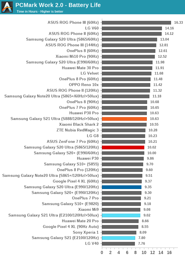
In terms of battery life in PCMark between the two phones, because we measured higher power draw on the Exynos, we naturally also see lower battery life on the new Samsung chip compared to the Snapdragon 888 variant of the S21 Ultra. The battery life here is tested in our traditional fashion, with the screen calibrated to 200cd/m² brightness.
The Snapdragon 888 S21 Ultra here fares better than the Galaxy S20 Ultra in terms of battery life, but by a quite minor amount. These results aren’t exactly great given the S21 Ultra’s massively more advanced and more efficient display.
For the Exynos 2100 S21 Ultra, the battery results here are actually slightly worse than the Exynos 990 S20 Ultra. This means that despite the new much more efficient screen, the Exynos 2100 is so aggressive in terms of performance scaling, that it draws notably more average power than the Exynos 990. Yes, the Exynos 2100 is also significantly more performant than its predecessor and this is immediately visible in terms of device usage, but it’s performance that wasn’t just achieved through efficiency, but also through more power usage.
We also got a smaller S21 with the Exynos 2100 – this variant as well as the S21+ do not have the new super-efficient OLED screen the S21 Ultra has, and as such the SoC’s more aggressive power draw is more prominently showcased through quite bad power efficiency in this test at 120Hz.
As we spend more times with the devices, we’ll be completing the test numbers at 60Hz as well as getting data from our web-browsing test. For the time being, the general view is that these new SoCs showcase quite increased performance, however their power draw has also gone up – meaning that battery life generationally should actually go down – with the exception of other non-SoC factors such as the S21 Ultra’s new more efficient display panel.
Moving onto the GPU side of things, I was very intrigued coming into this comparison, as both Qualcomm as well as Samsung LSI had made promises of enormous performance upgrades in the range of 35% and 40% respectively. We didn’t exactly know how Qualcomm achieved these performance gains given this year’s rather opaquer reveal of the Snapdragon 888. On the Exynos side, I was immediately dubious about Samsung’s 40% claim given that the new Mali-G78 was only meant to be a small generational performance and efficiency boost, as well as the process node having only a 20% power efficiency gain, however the Exynos 990 was in a bad position so maybe it was possible to achieve. Given a lack of large architectural as well as process node improvements, the large performance improvements must thus come from large power increases.
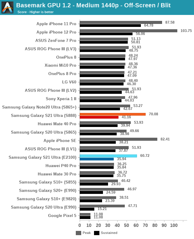
Starting off with Basemark GPU, we’re off to a mixed start. Both the Snapdragon 888 and Exynos 2100 notably outperform their predecessors in terms of peak performance, however their sustained performances on the Galaxy S21 Ultra isn’t too great.
The Exynos 2100 improves dramatically over the Exynos 990 in this regard, however the Snapdragon 888 S21 barely budges the needle against its predecessor, posting roughly the same sustained performance figures as any other Snapdragon 865 device such as the S20 Ultra.
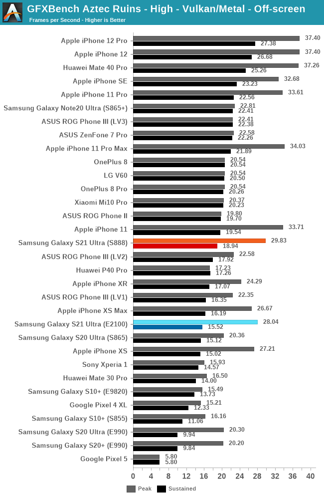
In GFXBench Aztec High, we see a similar story, where peak performance of both phones is much greater than before, however it quickly throttles onto mediocre figures. Again, these are still great improvements for the Exynos, but not so great figures for the Snapdragon 888 S21 Ultra, as it’s posting worse figures than the Note20 Ultra with the Snapdragon 865+.
| GFXBench Aztec High Offscreen Power Efficiency (System Active Power) |
||||
| Mfc. Process | FPS | Avg. Power (W) |
Perf/W Efficiency |
|
| iPhone 12 Pro (A14) 🔥 Throttled | N5 | 28.36 | 3.91 | 7.24 |
| Mate 40 Pro (Kirin 9000) 🔋 Power-Save | N5 | 23.71 | 3.35 | 7.07 |
| iPhone 11 Pro (A13) 🔥 Throttled | N7P | 26.14 | 3.83 | 6.82 |
| Galaxy S21U (Snapdragon 888) 🔥 Throttled | 5LPE | 18.94 | 2.81 | 6.71 |
| iPhone 12 Pro (A14) ❄️ Peak | N5 | 37.40 | 5.57 | 6.64 |
| iPhone 11 Pro (A13) ❄️ Peak | N7P | 34.00 | 6.21 | 5.47 |
| Galaxy S20U (Snapdragon 865) | N7P | 20.35 | 3.91 | 5.19 |
| Mate 40 Pro (Kirin 9000) 🔥 Throttled | N5 | 27.37 | 5.39 | 5.07 |
| iPhone XS (A12) 🔥 Throttled | N7 | 19.32 | 3.81 | 5.07 |
| Reno3 5G (Dimensity 1000L) | N7 | 11.93 | 2.39 | 4.99 |
| Galaxy S21U (Exynos 2100) 🔥 Throttled | 5LPE | 18.55 | 3.73 | 4.96 |
| iPhone XS (A12) ❄️ Peak | N7 | 26.59 | 5.56 | 4.78 |
| Mate 40 Pro (Kirin 9000) ❄️ Peak | N5 | 37.22 | 8.53 | 4.36 |
| ROG Phone III (Snapdragon 865+) | N7P | 22.34 | 5.35 | 4.17 |
| Mate 30 Pro (Kirin 990 4G) | N7 | 16.50 | 3.96 | 4.16 |
| Galaxy S21U (Snapdragon 888) ❄️ Peak | 5LPE | 29.82 | 8.10 | 3.68 |
| Galaxy S21U (Exynos 2100) ❄️ Peak | 5LPE | 28.04 | 7.69 | 3.64 |
| Galaxy S20+ (Exynos 990) | 7LPP | 20.20 | 5.02 | 3.59 |
| Galaxy S10+ (Snapdragon 855) | N7 | 16.17 | 4.69 | 3.44 |
| Galaxy S10+ (Exynos 9820) | 8LPP | 15.59 | 4.80 | 3.24 |
In terms of power and power efficiency, red alert, red alert!
Both the Exynos 2100 and Snapdragon 888 are showcasing outrageous peak power figures around 8W, which are figures that are simply impossible to sustain or dissipate in a phone.
We can see that both chips are way beyond their predecessors points in the frequency/voltages curves as the power efficiency is either outright flat, for the Exynos, or worse than their predecessors, like the Snapdragon – meaning both chips are using exponentially more power to try to drive more performance.
The phones quickly throttle down to below 4W – and fluctuate lower or higher depending on your environmental conditions. I was able to get power measurements for the Exynos around the 4W range (though it throttles down to below that), however for the Snapdragon this wasn’t possible as the phone’s thermal management had a very binomial behaviour of either settling at 3W power or ramping up to 6W, with very little inbetween.
Still, at these different power measurement points, we coincidentally ended up with similar performance – with the Snapdragon 888 here taking the lead in efficiency by 35%.
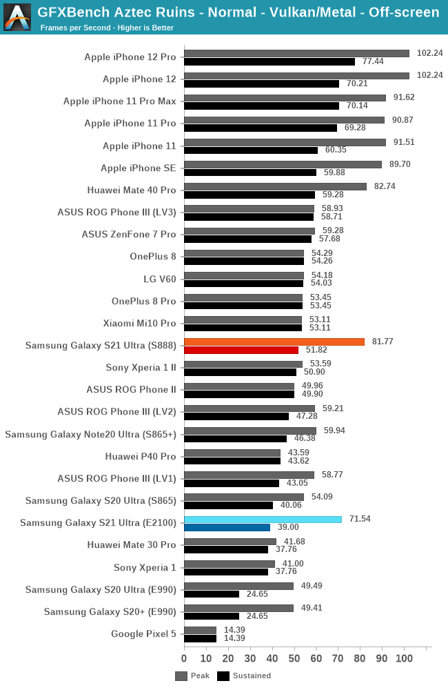
The 1080p variant of Aztec largely looks the same in terms of ranking, with the Exynos 2100 posting a good generational upgrade in sustained performance, while the Snapdragon 888 shows smaller gains.
| GFXBench Aztec Normal Offscreen Power Efficiency (System Active Power) |
||||
| Mfc. Process | FPS | Avg. Power (W) |
Perf/W Efficiency |
|
| iPhone 12 Pro (A14) 🔥 Throttled | N5 | 77.44 | 3.88 | 19.95 |
| iPhone 12 Pro (A14) ❄️ Peak | N5 | 102.24 | 5.53 | 18.48 |
| iPhone 11 Pro (A13) 🔥 Throttled | N7P | 73.27 | 4.07 | 18.00 |
| Galaxy S21U (Snapdragon 888) 🔥 Throttled | 5LPE | 51.81 | 2.93 | 17.67 |
| Mate 40 Pro (Kirin 9000) 🔋 Power-Save | N5 | 53.49 | 3.10 | 17.25 |
| iPhone 11 Pro (A13) ❄️ Peak | N7P | 91.62 | 6.08 | 15.06 |
| iPhone XS (A12) 🔥 Throttled | N7 | 55.70 | 3.88 | 14.35 |
| Galaxy S20U (Snapdragon 865) | N7P | 54.09 | 3.91 | 13.75 |
| iPhone XS (A12) ❄️Peak | N7 | 76.00 | 5.59 | 13.59 |
| Reno3 5G (Dimensity 1000L) | N7 | 27.84 | 2.12 | 13.13 |
| Galaxy S21U (Exynos 2100) 🔥 Throttled | 5LPE | 46.29 | 3.85 | 12.02 |
| Mate 40 Pro (Kirin 9000) 🔥 Throttled | N5 | 63.56 | 5.37 | 11.84 |
| ROG Phone III (Snapdragon 865+) | N7P | 58.77 | 5.34 | 11.00 |
| Mate 40 Pro (Kirin 9000) ❄️ Peak | N5 | 82.74 | 7.95 | 10.40 |
| Mate 30 Pro (Kirin 990 4G) | N7 | 41.68 | 4.01 | 10.39 |
| Galaxy S20+ (Exynos 990) | 7LPP | 49.41 | 4.87 | 10.14 |
| Galaxy S10+ (Snapdragon 855) | N7 | 40.63 | 4.14 | 9.81 |
| Galaxy S21U (Snapdragon 888) ❄️ Peak | 5LPE | 81.77 | 8.40 | 9.73 |
| Galaxy S20U (Exynos 2100) ❄️ Peak | 5LPE | 71.53 | 8.10 | 8.83 |
| Galaxy S10+ (Exynos 9820) | 8LPP | 40.18 | 4.62 | 8.69 |
In terms of power, here’s it’s even higher, with the Snapdragon doing one run at 8.4W of power.
Throttling down, the Snapdragon 888 takes the lead in terms of efficiency as seemingly it has a differently shaped power curve and benefits more at lower frequencies.
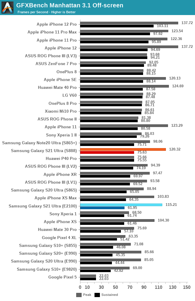
Same story in Manhattan – good upgrades for the Exynos 2100 – although still not very competitive, while the Snapdragon 888 is flat against most other Snapdragon 865 phones.
| GFXBench Manhattan 3.1 Offscreen Power Efficiency (System Active Power) |
||||
| Mfc. Process | FPS | Avg. Power (W) |
Perf/W Efficiency |
|
| iPhone 12 Pro (A14) 🔥 Throttled | N5 | 103.11 | 3.90 | 26.43 |
| Galaxy S21U (Snapdragon 888) 🔥 Throttled | 5LPE | 75.62 | 2.91 | 25.98 |
| iPhone 12 Pro (A14) ❄️ Peak | N5 | 137.72 | 5.63 | 24.46 |
| iPhone 11 Pro (A13) 🔥 Throttled | N7P | 100.58 | 4.21 | 23.89 |
| Mate 40 Pro (Kirin 9000) 🔋 Power-Save | N5 | 95.01 | 4.35 | 21.83 |
| Galaxy S20U (Snapdragon 865) | N7P | 88.93 | 4.20 | 21.15 |
| iPhone 11 Pro (A13) ❄️Peak | N7P | 123.54 | 6.04 | 20.45 |
| iPhone XS (A12) 🔥 Throttled | N7 | 76.51 | 3.79 | 20.18 |
| Reno3 5G (Dimensity 1000L) | N7 | 55.48 | 2.98 | 18.61 |
| Galaxy S21U (Exynos 2100) 🔥 Throttled | 5LPE | 72.66 | 4.04 | 17.98 |
| Mate 40 Pro (Kirin 9000) 🔥 Throttled | N5 | 87.31 | 4.98 | 17.54 |
| iPhone XS (A12) ❄️Peak | N7 | 103.83 | 5.98 | 17.36 |
| ROG Phone III (Snapdragon 865+) | N7P | 93.58 | 5.56 | 16.82 |
| Galaxy S20U (Exynos 2100) ❄️ Peak | 5LPE | 115.20 | 7.62 | 15.11 |
| Mate 40 Pro (Kirin 9000) ❄️Peak | N5 | 124.69 | 8.28 | 15.05 |
| Mate 30 Pro (Kirin 990 4G) | N7 | 75.69 | 5.04 | 15.01 |
| Galaxy S20+ (Exynos 990) | 7LPP | 85.66 | 5.90 | 14.51 |
| Galaxy S10+ (Snapdragon 855) | N7 | 70.67 | 4.88 | 14.46 |
| Galaxy S21U (Snapdragon 888) ❄️ Peak | 5LPE | 120.32 | 8.34 | 14.42 |
| Galaxy S10+ (Exynos 9820) | 8LPP | 68.87 | 5.10 | 13.48 |
| Galaxy S9+ (Snapdragon 845) | 10LPP | 61.16 | 5.01 | 11.99 |
| Mate 20 Pro (Kirin 980) | N7 | 54.54 | 4.57 | 11.93 |
| Galaxy S9 (Exynos 9810) | 10LPP | 46.04 | 4.08 | 11.28 |
| Galaxy S8 (Snapdragon 835) | 10LPE | 38.90 | 3.79 | 10.26 |
| Galaxy S8 (Exynos 8895) | 10LPE | 42.49 | 7.35 | 5.78 |
In terms of power and efficiency, at peak performance the Snapdragon 888 here actually seems to be fare off worse: it’s posting slightly more FPS, however It’s also higher power, reaching up to 8.34W.
Throttling down again shows that the Snapdragon has a steeper power curve and becomes more efficient at lower frequency points. The throttled states of both phones post nearly the same performance, but the Snapdragon does it at 28% lower power.
| GFXBench T-Rex Offscreen Power Efficiency (System Active Power) |
||||
| Mfc. Process | FPS | Avg. Power (W) |
Perf/W Efficiency |
|
| iPhone 12 Pro (A14) 🔥 Throttled | N5 | 260.28 | 4.08 | 63.97 |
| Galaxy S21U (Snapdragon 888) 🔥 Throttled | 5LPE | 172.67 | 2.70 | 63.74 |
| iPhone 11 Pro (A13) 🔥 Throttled | N7P | 289.03 | 4.78 | 60.46 |
| iPhone 12 Pro (A14) ❄️ Peak | N5 | 328.50 | 5.55 | 59.18 |
| iPhone 11 Pro (A13) ❄️ Peak | N7P | 328.90 | 5.93 | 55.46 |
| Galaxy S20U (Snapdragon 865) | N7P | 205.37 | 3.83 | 53.30 |
| Mate 40 Pro (Kirin 9000) 🔥 Throttled | N5 | 147.13 | 2.92 | 50.38 |
| iPhone XS (A12) 🔥 Throttled | N7 | 197.80 | 3.95 | 50.07 |
| Mate 40 Pro (Kirin 9000) 🔋 Power-Save | N5 | 201.85 | 4.10 | 49.22 |
| ROG Phone III (Snapdragon 865+) | N7P | 224.48 | 4.92 | 45.60 |
| iPhone XS (A12) ❄️Peak | N7 | 271.86 | 6.10 | 44.56 |
| Galaxy 10+ (Snapdragon 855) | N7 | 167.16 | 4.10 | 40.70 |
| Galaxy S21U (Exynos 2100) 🔥 Throttled | 5LPE | 153.28 | 3.80 | 40.30 |
| Reno3 5G (Dimensity 1000L) | N7 | 139.30 | 3.57 | 39.01 |
| Mate 40 Pro (Kirin 9000) ❄️ Peak | N5 | 235.04 | 6.11 | 38.46 |
| Galaxy S20+ (Exynos 990) | 7LPP | 199.61 | 5.63 | 35.45 |
| Mate 30 Pro (Kirin 990 4G) | N7 | 152.27 | 4.34 | 35.08 |
| Galaxy S21U (Snapdragon 888) ❄️ Peak | 5LPE | 279.39 | 7.98 | 35.01 |
| Galaxy S9+ (Snapdragon 845) | 10LPP | 150.40 | 4.42 | 34.00 |
| Galaxy 10+ (Exynos 9820) | 8LPP | 166.00 | 4.96 | 33.40 |
| Galaxy S9 (Exynos 9810) | 10LPP | 141.91 | 4.34 | 32.67 |
| Galaxy S8 (Snapdragon 835) | 10LPE | 108.20 | 3.45 | 31.31 |
| Galaxy S20U (Exynos 2100) ❄️ Peak | 5LPE | 237.71 | 8.02 | 29.61 |
| Mate 20 Pro (Kirin 980) | N7 | 135.75 | 4.64 | 29.25 |
| Galaxy S8 (Exynos 8895) | 10LPE | 121.00 | 5.86 | 20.65 |
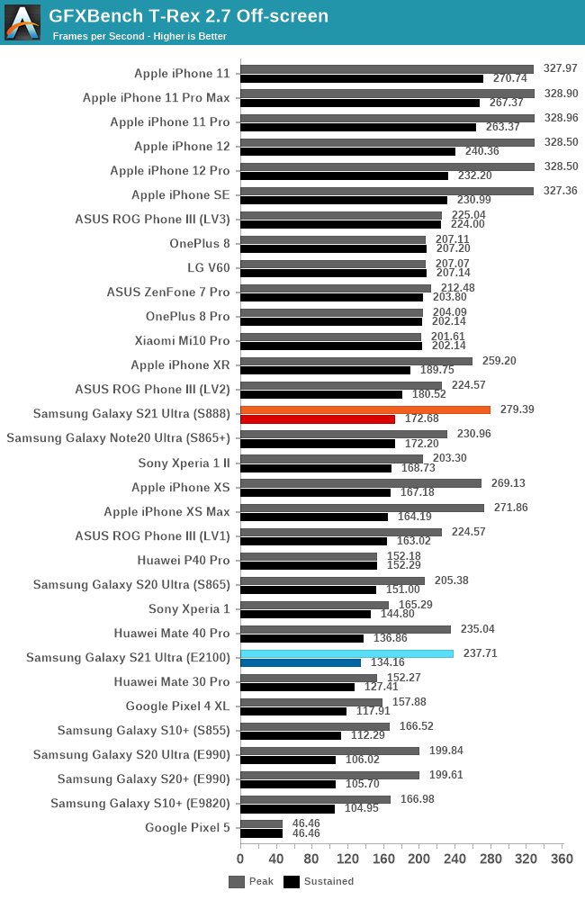
Finally, in T-Rex, the Snapdragon takes a more significant lead in peak performance at the same power, while when throttled down, the Adreno GPU showcases a +50% advantage in perf/W.
Much Too Hot to Handle
I’ll be quite frank with the results of these new SoCs: they’re terrible. Much like smartphone vendors have for years now copied the worst aspects of Apple’s devices, such a dropping headphone jacks and dropping chargers, the SoC vendors this year have now also copied the worst aspect of Apple’s SoCs: extremely high GPU peak power states.
When I tested the Kirin 9000 a few months ago in the Mate 40 Pro I thought that HiSilicon’s choice of turbocharging their massive GPU up to peak power figures of 8W was a very bad choice, but now Qualcomm and Samsung LSI followed up doing the exactly same thing, as if this was a race to the bottom as to who can create the hottest GPU in the market.
As to why the SoC vendors are doing this, it’s very easy to look at the benchmark charts and see the marketing pressure that Apple applies on the rest of the industry, being far ahead of the pack in terms of performance and efficiency. I wouldn’t be surprised if this generation of SoCs have had design decisions impacted by the marketing departments.
Inside devices such as the Galaxy S21 Ultra today – these peak performance states are utterly pointless as they are just impossible to maintain for any reasonable amount of time, as the thermal envelope of the phones really aren’t any different to that of any other device of this form-factor, including the predecessor S20 Ultra.
The Snapdragon 888’s peak performance state is pretty absurd, as at its 840MHz GPU frequency I’ve measured average power of a round 11W. This state can’t be maintained for longer than a few seconds before it throttles down to 778 and 738MHz at 9-8W for the rest of the duration of a test on a cold device, before further limiting down due to thermals during prolonged periods. In terms of sustained performance, the S21U’s advantages over the S20U is in the 5-20% range, depending on workload, well below Qualcomm’s proclaimed 35% performance boost. That margin here actually is even smaller against the Snapdragon 865+ Galaxy Note20 Ultra.
I asked Qualcomm to rationalise these high-wattage peak performance points, and the official response was that these were enabled in order to give a higher level of flexibility in terms of higher power gaming phones and higher thermal envelope devices which are able to sustain greater power levels. I know that at least Xiaomi’s Mi 11 will be more aggressive than the S21 Ultra in terms of sustained power levels, at a cost of higher device temperatures. As for gaming phones – the last few generation of those devices have shown little actual physical design differentiation to actually enable higher thermal envelopes, with most of their advantages simply being that they are allowed to get hotter, showing no advantage over “regular” phones which do the same (OnePlus devices, ZenFone 7 Pro for example). The S21 Ultra here has peak skin temperatures of around 46°C with long-term throttling at around 42°C.
For the Exynos 2100 – Samsung LSI’s claim of a 40% performance boost is more credible as this not only refers to the peak performance figures, but can actually also be applied to the sustained performance figures of the phone. It’s actually a tangible and very large upgrade to the Exynos 990 last year, however it needs to be put into context. The peak power figures here have the same negative connotations as on the Snapdragon unit so I won’t repeat myself in that aspect.
In terms of sustained performance, although the Exynos 2100 is a large generational upgrade, it still falls below that of last-generation Snapdragon 865 devices, and naturally also the newer Snapdragon 888. The benchmark figures here also pretty much correspond to the real-world gaming performance of the phones – the Exynos S21 Ultra fared not only worse than the Snapdragon S21 Ultra, but also worse than a Snapdragon S20 Ultra or Note20 Ultra.
The interesting data here is the comparison to Huawei’s Mate 40 Pro with the Kirin 9000 and its gargantuan Mali-G78MP24 GPU – 10 more cores than the Exynos 2100’s configuration. Putting the Mate 40 Pro into power-saving mode will actually cap the maximum GPU frequency and give you reasonable power consumption figures around 4W, which are comparable to what the Exynos 2100 in the S21 Ultra throttles at. We can see that the Kirin’s performance is either superior, lower power, or both, signifying the chip is being notably more efficient than the Exynos 2100. The larger GPU as well as the superior TSMC 5nm node come at play here.
Samsung LSI’s confirmation that they’ll be deploying AMD’s RDNA-based GPU for next-generation flagship SoCs will hopefully mean that the Exynos’ competitive positioning will be quite different next year; however, we shouldn’t expect miracles as the process node differences to Apple’s GPUs will likely still linger on.
Unfortunately, Samsung’s (the mobile division) battery saving mode on the Galaxy S21 doesn’t affect the GPU frequencies at all, unlike Huawei’s PSM, so it doesn’t help at all for the power envelopes or efficiency. I would highly recommend them to introduce such a mechanism here as having burning hot phones really isn’t a great experience while gaming, and the performance will regress to those sustained levels anyhow.
Generally, I see this generation as quite the disappointment when it comes to GPU advancements. Qualcomm likely suffered an efficiency set-back and minor improvements due to the process node shift, and while Samsung LSI has achieved good generational advancements, the Exynos still clearly falls behind due to architectural GPU disadvantages.
It’s been a tumultuous and busy week as we’ve only had the new Galaxy S21 Ultra in Snapdragon and Exynos variants for just a few days now, but that’s sufficient as we can generally come to a representative conclusion as to how Qualcomm’s and Samsung’s new generation flagship SoCs will play out in 2021 – and for the most part, it’s probably not what people were expecting.
Starting off with the most hyped up part of the new SoCs (mea culpa), both SoCs are the first to employ Arm’s newest Cortex-X1 cores, the first CPU generation in which Arm really went for a more “performance first” design philosophy. In general, the new CPU IP does live up to its claims, however Arm’s and our own performance projections weren’t met by the new SoCs, as they didn’t quite reach the configurations and clock frequencies we had hoped for 2021 designs. Both Qualcomm and Samsung didn’t invest on an 8MB L3 cache, and in particular Samsung didn’t even don their X1 core with a full 1MB of L2 cache. This does seem to be noticeable in the performance as the Snapdragon 888 does have small performance edge over the Exynos 2100. Samsung’s choice here given their years of wasting lots of silicon on humongous custom CPUs seems to be rather puzzling, but generally both vendors aren’t as aggressive as Apple is on investing die area into caches.
Qualcomm still has a clear memory subsystem advantage as the company has made large strides in latency this generation, and this results in even more extra performance. The Exynos this year surprised us with a much larger system level cache – which however seems to also add to latency and reduce performance.
More worrisome for the Exynos is its weird clock behaviour, with the new chip really struggling in maintaining its peak frequencies other than for very brief moments – the Snapdragon 888’s X1 core had no such issues. My Exynos S21 Ultra chip bin was quite terrible here, but the better silicon on my second S21 doesn’t improve things too much either.
The Exynos 2100’s Cortex-A78 cores are clocked higher than the Snapdragon 888’s, and this show up in performance, however in every-day workloads the DVFS of the Exynos actually behaves more similarly to the Snapdragon as it generally scales things to 2600MHz and only uses the 2808MHz peak frequencies of these cores in brief multi-threaded workloads, as long as thermals even allow it, as even these middle cores can get quite power hungry this generation.
Although both are using the same IP on the same process node, the Exynos 2100’s CPU just look to be more power hungry than the Snapdragon 888’s implementations. Given the apples-to-apples comparison, the only remaining possibility is just a weaker physical design implementation on Samsung LSI’s part – which is actually a point of concern, as we had hoped Exynos SoCs would catch up this year following their ditching of their custom CPU cores. Make no mistake – the new X1 cores are massively improved in performance and efficiency over last year’s M5 cores, it’s just that Qualcomm shows that it can be done even better.
On the GPU side of things, this generation feels wrong to me, and that’s solely due to the peak power levels these new SoCs reach, and which vendors actually left enabled in commercial devices.
Qualcomm had advertised 35% improved GPU performance this generation with the Snapdragon 888, and that might indeed be valid for peak performance, but certainly for Samsung devices that figure is absolutely unreachable for any reasonable amount of gaming periods, as the power consumption is through the roof at over 8W. I don’t see how other vendors might be able to design phones with thermal dissipations that allows for such power levels to actually be maintained without the phone’s skin temperatures exceeding +50°C (122°F), it’s just utterly pointless in my opinion.
In terms of sustained performance, the Snapdragon 888 is generally a 10-15% improvement over the Snapdragon 865 and 865+ - at least in these Samsung devices whose thermal limits and thermal envelopes are similar this generation, attempting to target 42°C peak skin temperatures, although the phones failed to stay below that threshold during the initial few minutes of the performance burn.
On the Exynos 2100 side, Samsung’s +40% performance claim can be considered accurate just for the fact that it generally applies to both peak and sustained performance figures. At peak performance, the SoC is just as absurd at 8W load, which is impossible to maintain. The good news here though, is that when throttling down, the Exynos 2100 is notably better than the Exynos 990 – however that’s not sufficient to catch up to last year’s Snapdragon 865, much less the new Snapdragon 888.
Samsung’s 5LPE process appears to be lacking
We don’t have deeper technical insights as to how Samsung’s process node compares in relation to TSMC’s nodes other than the actual performance of the chips we have in ours hands, so I’m basing my arguments based on the measured data that I’m seeing here.
At lower performance levels, we noted that the 5LPE node doesn’t look to be any different than TSMC’s N7P node, as the A55 cores in the Snapdragon 888 performed and used up exactly the same amount of power as in the Snapdragon 865. At higher performance levels however, we’re seeing regressions – the middle Cortex-A78 cores of the S888 should have been equal power, or at least similar, to the identically clocked A77 cores of the S865, however we’re seeing a 25% power increase this generation.
Similarly, in theory, the Exynos 2100 Cortex-A78 cores at 2.81GHz should have been somewhat similar in power to the 2.84GHz A77 cores of a Snapdragon 865, but it’s again at a 20-25% disadvantage in efficiency.
In fact, both SoCs on the CPU side don’t seem to be able to reach the Kirin 9000’s lower power levels and efficiency even though that chip is running at 3.1GHz – it’s clear to me that TSMC’s N5 node is quite superior in terms of power efficiency.
There are two conclusions here: For Samsung’s Exynos 2100 – it doesn’t really change the situation all that much. 5LPE does seem to be better than 7LPP, and the new chip is definitely more energy efficient than the Exynos 990 – although it does look that the new much more aggressive behaviour of the CPUs, while benefiting performance, can have an impact on battery life. We need more time with the phones to get to a definitive conclusion in that regard.
For Qualcomm’s Snapdragon 888, the new chip’s manufacturing seems to be giving it headwinds. At best, we’re seeing flat energy efficiency, and at worst, we’re seeing generational regressions. This all depends on the operating point, but generally, the new chip seems to be slightly more power hungry than its predecessor – although again, performance has indeed improved. On the CPU side, the performance boost could be noticeable, but more problematic is the sustained GPU performance increase, which is still quite minor. It’s at this point where we have to talk about things other than CPU and GPU, such as Qualcomm’s new Hexagon accelerator, or new camera and ISP capabilities. We weren’t able to test the AI/NPUs today as the software frameworks on the S21 Ultra aren’t complete so it’s something we’ll have to revisit in the future. Looking at all these results, it suddenly makes sense as to why Qualcomm launched another bin/refresh of the Snapdragon 865 in the form of the Snapdragon 870.
Overall, this generation seems a bit lacklustre. Samsung LSI still has work ahead of them in improving fundamental aspects of the Exynos SoCs, maturing the CPU cluster integration with the memory subsystem and adopting AMD’s RDNA architecture GPU in the next generation seem two top items on the to-do list for the next generation, along with just general power efficiency improvements. Qualcomm, while seemingly having executed things quite well this generation, seem to be limited by the process node. We can’t really blame them for this if they couldn’t get the required TSMC volume, but it also means we’re nowhere near in closing the gap with Apple’s SoCs.
In general, I’m sure this year’s devices will be good – but one should have tapered expectations. We'll be following up with full device reviews of the Galaxy S21 Ultras as well as the smaller Galaxy S21 soon - so stay tuned.
https://ift.tt/3d40SB5
Technology
Bagikan Berita Ini


0 Response to "The Snapdragon 888 vs The Exynos 2100: Cortex-X1 & 5nm - Who Does It Better? - AnandTech"
Post a Comment